Material, Technologie
& Kristalle GmbH
& Kristalle GmbH
Ihre Verbindung zu uns

-
 English
-
Deutsch
Warenkorb
0
Artikel
Artikel
Keine Artikel
0,00 €
Gesamt
Gesamt zzgl. MwSt.
Artikel wurde in den Korb gelegt
Menge
Sie haben 0 Artikel in Ihrem Warenkorb.
Es gibt 1 Artikel in Ihrem Warenkorb.
Versandkosten (o. MwSt.)
noch festzulegen
Gesamt
(o. MwSt.)


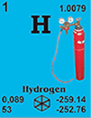
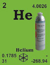
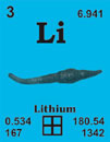
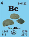
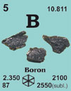
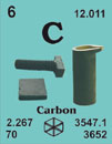
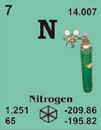
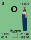
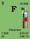
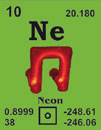
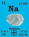
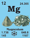
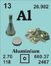
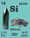
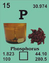
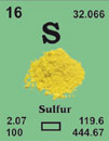
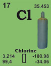
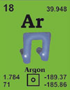
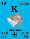
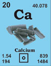
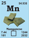
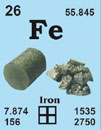
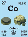
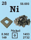
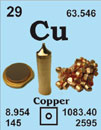
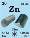
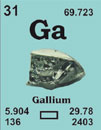
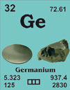
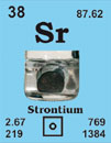
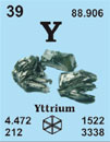
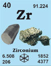
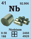
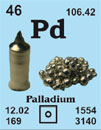
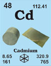
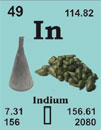
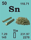
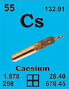
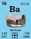
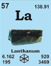
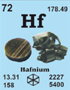
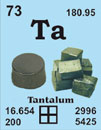
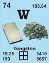
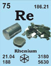
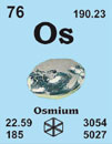
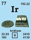
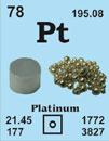
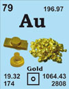
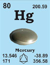
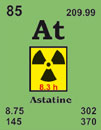
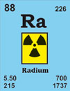
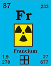
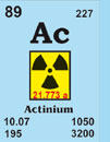
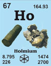
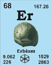
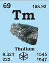
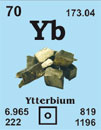
Übersicht der Elemente mit Zugang zu unserem Shop


Tel.: +49 (0) 2461 - 9352 - 0
Fax: +49 (0) 2461 - 9352 - 11
Fax: +49 (0) 2461 - 9352 - 11